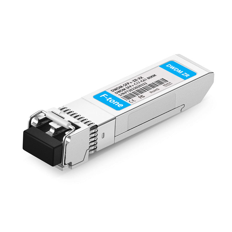
Features:
- Supports 9.95 to 11.3Gb/s bit rates
- Hot-Pluggable
- Duplex LC connector
- DWDM TUNABLE laser transmitter
- APD photo-detector
- 50GHz ITU-T Grid, C Band
- SMF links up to 80km
- 2-wire interface for management specifications compliant with SFF 8472 digital diagnostic monitoring interface
- Power Supply :+3.3V
- Power consumption<2.5W
- Temperature Range: 0~ 70°C
- RoHS compliant
Applications:
- Fully Tunable 50GHz DWDM SFP
- 10GBASE-ZR/ZW Ethernet
- Sonet OC-192/SDH SDH STM-64 ITU-T G.959.1 P1L1-2D2
- 10G Fibre channel
- DWDM Networks
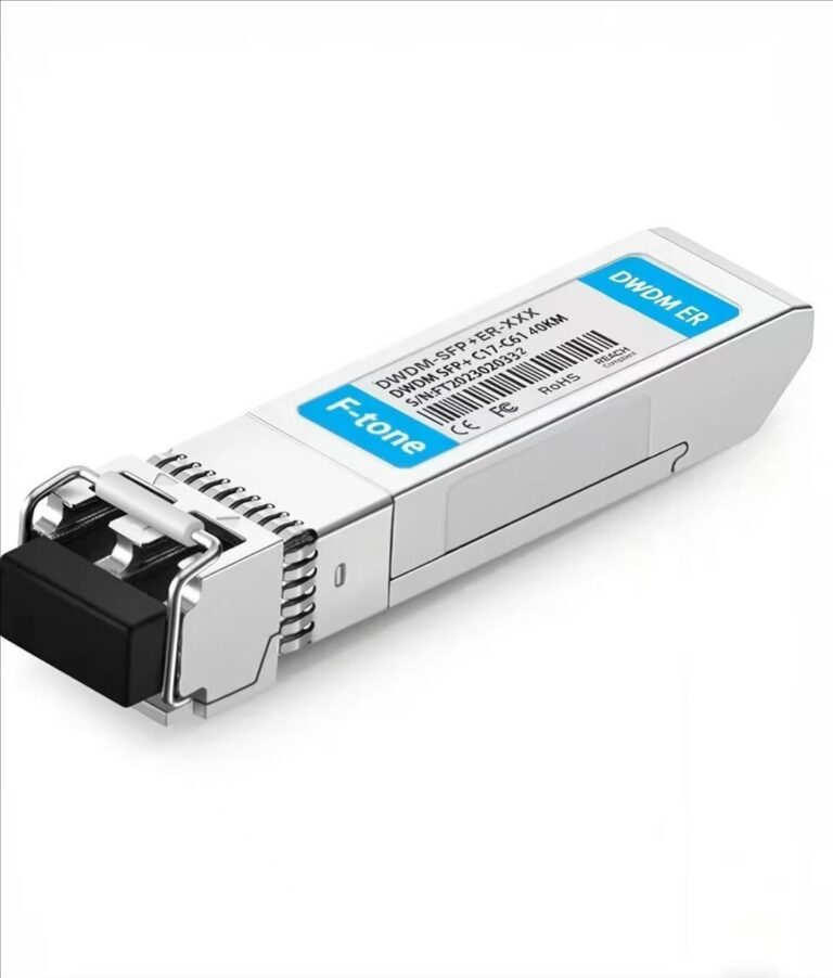
FSPD-10GD80-T50
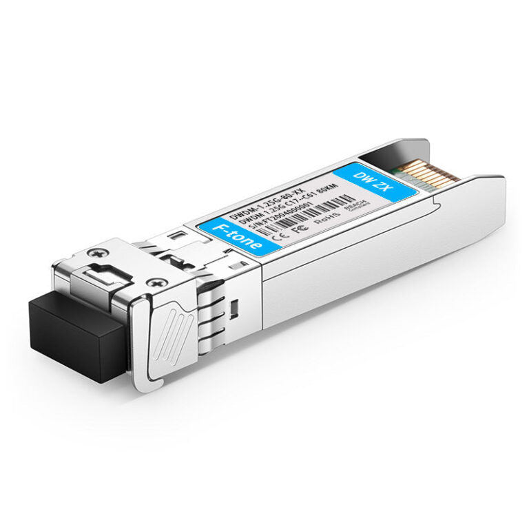
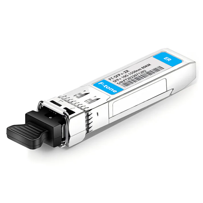
10Gb/s 80km DWDM Tunable SFP Transceiver
Hot Pluggable, Duplex LC, 50GHz ITU-T-T, DWDM Tunable&APD, Single mode
Description:
F-tone’ FSPD-10GD80-T50 Small Form Factor 10Gb/s (SFP) transceivers are compliant with the current SFP Multi-Source Agreement (MSA) Specification. The high performance cooled DWDM TUNABLE transmitter and high sensitivity APD receiver provide superior performance for SONET/SDH, 10G FC and Ethernet applications up to 80km optical links.
The SFP+ Module compliants with SFF-8431, SFF-8432 and IEEE 802.3ae 10GBASE-ZR. Digital diagnostics functions are available via a 2-wire serial interface, as specified in SFF-8472.
The fully SFP compliant form factor provides hot pluggability, easy optical port upgrades and low EMI emission.
- Absolute Maximum Ratings
|
Parameter |
Symbol |
Min. |
Typical |
Max. |
Unit |
|
Storage Temperature |
TS |
-40 |
|
+85 |
°C |
|
Case Operating Temperature |
TA |
0 |
|
70 |
°C |
|
Maximum Supply Voltage |
Vcc |
-0.5 |
|
4 |
V |
|
Relative Humidity |
FH |
0 |
|
85 |
% |
- Electrical Characteristics (TOP = 0 to 70 °C, VCC = 3.135 to 3.465 Volts)
|
Parameter |
Symbol |
Min. |
Typical |
Max. |
Unit |
Note |
|
Supply Voltage |
Vcc |
3.135 |
|
3.465 |
V |
|
|
Supply Current |
Icc |
|
350 |
450 |
mA |
|
|
Power Consumption |
P |
|
|
1.5 |
W |
|
|
Transmitter Section: |
||||||
|
Input differential impedance |
Rin |
|
100 |
|
Ω |
1 |
|
Tx Input Single Ended DC Voltage Tolerance (Ref VeeT) |
V |
-0.3 |
|
4 |
V |
|
|
Differential input voltage swing |
Vin,pp |
180 |
|
700 |
mV |
2 |
|
Transmit Disable Voltage |
VD |
2 |
|
Vcc |
V |
3 |
|
Transmit Enable Voltage |
VEN |
Vee |
|
Vee+0.8 |
V |
|
|
Receiver Section: |
||||||
|
Single Ended Output Voltage Tolerance |
V |
-0.3 |
|
4 |
V |
|
|
Rx Output Diff Voltage |
Vo |
300 |
|
850 |
mV |
|
|
Rx Output Rise and Fall Time |
Tr/Tf |
30 |
|
|
ps |
4 |
|
LOS Fault |
VLOS fault |
2 |
|
VccHOST |
V |
5 |
|
LOS Normal |
VLOS norm |
Vee |
|
Vee+0.8 |
V |
5 |
Note:
1. Connected directly to TX data input pins. AC coupling from pins into laser driver IC.
2. Per SFF-8431 Rev 3.0
3. Into 100 ohms differential termination.
4. 20%~80%
5. LOS is an open collector output. Should be pulled up with 4.7k – 10kΩ on the host board. Normal operation is logic 0; loss of signal is logic 1. Maximum pull-up voltage is 5.5V.
- Optical Parameters(TOP = 0 to 70°C, VCC = 3.135 to 3.465 Volts)
|
Parameter |
Symbol |
Min. |
Typical |
Max. |
Unit |
Note |
|
Transmitter Section: |
||||||
|
Optical Wavelength-End Of Life |
λ |
X-100 |
X |
X+100 |
pm |
|
|
Optical Wavelength-Beginning Of Life |
λ |
X-25 |
X |
X+25 |
pm |
|
|
Average Optical Power |
Pavg |
0 |
|
+5 |
dBm |
1 |
|
Laser Off Power |
Poff |
|
|
-30 |
dBm |
|
|
Extinction Ratio |
ER |
6 |
|
|
dB |
|
|
Transmitter Dispersion Penalty |
TDP |
|
|
3.0 |
dB |
2 |
|
Relative Intensity Noise |
Rin |
|
|
-128 |
dB/Hz |
3 |
|
Optical Return Loss Tolerance |
|
20 |
|
|
dB |
|
|
Receiver Section: |
||||||
|
Center Wavelength |
λr |
1480 |
|
1565 |
nm |
|
|
Receiver Sensitivity |
Sen |
|
|
-23 |
dBm |
4 |
|
Los Assert |
LOSA |
-40 |
|
– |
dBm |
|
|
Los Dessert |
LOSD |
|
|
-24 |
dBm |
|
|
Los Hysteresis |
LOSH |
0.5 |
|
|
dB |
|
|
Overload |
Sat |
-7 |
|
|
dBm |
5 |
|
Receiver Reflectance |
Rrx |
|
|
-12 |
dB |
|
Note:
1. Average power figures are informative only, per IEEE802.3ae.
2. TWDP figure requires the host board to be SFF-8431compliant. TWDP is calculated using the Matlab code provided in clause 68.6.6.2 of IEEE802.3ae.
3. 12dB reflection.
4. Conditions of stressed receiver tests per IEEE802.3ae. CSRS testing requires the host board to be SFF-8431 compliant.
5. Receiver overload specified in OMA and under the worst comprehensive stressed condition.
- Timing Characteristics
|
Parameter |
Symbol |
Min. |
Typical |
Max. |
Unit |
|
TX_Disable Assert Time |
t_off |
|
|
10 |
us |
|
TX_Disable Negate Time |
t_on |
|
|
1 |
ms |
|
Time to Initialize Include Reset of TX_FAULT |
t_int |
|
|
300 |
ms |
|
TX_FAULT from Fault to Assertion |
t_fault |
|
|
100 |
us |
|
TX_Disable Time to Start Reset |
t_reset |
10 |
|
|
us |
|
Receiver Loss of Signal Assert Time |
TA,FX_LOS |
|
|
100 |
us |
|
Receiver Loss of Signal Deassert Time |
Td,FX_LOS |
|
|
100 |
us |
|
Rate-Select Chage Time |
t_ratesel |
|
|
10 |
us |
|
Serial ID Clock Time |
t_serial-clock |
|
|
100 |
kHz |
- Pin Assignment
Diagram of Host Board Connector Block Pin Numbers and Name
- Pin Function Definitions
|
PIN # |
Name |
Function |
Notes |
|
1 |
VeeT |
Module transmitter ground |
1 |
|
2 |
Tx Fault |
Module transmitter fault |
2 |
|
3 |
Tx Disable |
Transmitter Disable; Turns off transmitter laser output |
3 |
|
4 |
SDL |
2 wire serial interface data input/output (SDA) |
|
|
5 |
SCL |
2 wire serial interface clock input (SCL) |
|
|
6 |
MOD-ABS |
Module Absent, connect to VeeR or VeeT in the module |
2 |
|
7 |
FS0 |
Rate select0, optionally control SFP+ receiver. When high, input data rate >4.5Gb/ s; when low, input data rate <=4.5Gb/s |
|
|
8 |
LOS |
Receiver Loss of Signal Indication |
4 |
|
9 |
FS1 |
Rate select0, optionally control SFP+ transmitter. When high, input data rate >4.5Gb/s; when low, input data rate <=4.5Gb/s |
|
|
10 |
VeeR |
Module receiver ground |
1 |
|
11 |
VeeR |
Module receiver ground |
1 |
|
12 |
FT- |
Receiver inverted data out put |
|
|
13 |
FD+ |
Receiver non-inverted data out put |
|
|
14 |
VeeR |
Module receiver ground |
1 |
|
15 |
VccR |
Module receiver 3.3V supply |
|
|
16 |
VccT |
Module transmitter 3.3V supply |
|
|
17 |
VeeT |
Module transmitter ground |
1 |
|
18 |
TD+ |
Transmitter inverted data out put |
|
|
19 |
TD- |
Transmitter non-inverted data out put |
|
|
20 |
VeeT |
Module transmitter ground |
1 |
Note:
1. The module ground pins shall be isolated from the module case.
2. This pin is an open collector/drain output pin and shall be pulled up with 4.7K-10Kohms to Host_Vcc on the host board.
3. This pin shall be pulled up with 4.7K-10Kohms to VccT in the module.
4. This pin is an open collector/drain output pin and shall be pulled up with 4.7K-10Kohms to Host_Vcc on the host board.
- SFP Module EEPROM Information and Management
The SFP modules implement the 2-wire serial communication protocol as defined in the SFP -8472. The serial ID information of the SFP modules and Digital Diagnostic Monitor parameters can be accessed through the I2C interface at address A0h and A2h. The memory is mapped in Table 1. Detailed ID information (A0h) is listed in Table 2. And the DDM specification at address A2h. For more details of the memory map and byte definitions, please refer to the SFF-8472, “Digital Diagnostic Monitoring Interface for Optical Transceivers”. The DDM parameters have been internally calibrated.
Table 1. Digital Diagnostic Memory Map (Specific Data Field Descriptions)
Table 2 – EEPROM Serial ID Memory Contents (A0h)
|
Data Address |
Length (Byte) |
Name of Length |
Description and Contents |
|
Base ID Fields |
|||
|
0 |
1 |
Identifier |
Type of Serial transceiver (03h=SFP) |
|
1 |
1 |
Reserved |
Extended identifier of type serial transceiver (04h) |
|
2 |
1 |
Connector |
Code of optical connector type (07=LC) |
|
3-10 |
8 |
Transceiver |
10G Base-ZR |
|
11 |
1 |
Encoding |
64B/66B |
|
12 |
1 |
BR, Nominal |
Nominal baud rate, unit of 100Mbps |
|
13-14 |
2 |
Reserved |
(0000h) |
|
15 |
1 |
Length(9um) |
Link length supported for 9/125um fiber, units of 100m |
|
16 |
1 |
Length(50um) |
Link length supported for 50/125um fiber, units of 10m |
|
17 |
1 |
Length(62.5um) |
Link length supported for 62.5/125um fiber, units of 10m |
|
18 |
1 |
Length(Copper) |
Link length supported for copper, units of meters |
|
19 |
1 |
Reserved |
|
|
20-35 |
16 |
Vendor Name |
SFP vendor name: F-tone |
|
36 |
1 |
Reserved |
|
|
37-39 |
3 |
Vendor OUI |
SFP transceiver vendor OUI ID |
|
40-55 |
16 |
Vendor PN |
Part Number: “TSPLXG80D-T50” (ASCII) |
|
56-59 |
4 |
Vendor rev |
Revision level for part number |
|
60-62 |
3 |
Reserved |
|
|
63 |
1 |
CCID |
Least significant byte of sum of data in address 0-62 |
|
Extended ID Fields |
|||
|
64-65 |
2 |
Option |
Indicates which optical SFP signals are implemented (001Ah = LOS, TX_FAULT, TX_DISABLE all supported) |
|
66 |
1 |
BR, max |
Upper bit rate margin, units of % |
|
67 |
1 |
BR, min |
Lower bit rate margin, units of % |
|
68-83 |
16 |
Vendor SN |
Serial number (ASCII) |
|
84-91 |
8 |
Date code |
F-tone’s Manufacturing date code |
|
92-94 |
3 |
Reserved |
|
|
95 |
1 |
CCEX |
Check code for the extended ID Fields (addresses 64 to 94) |
|
Vendor Specific ID Fields |
|||
|
96-127 |
32 |
Readable |
F-tone specific date, read only |
|
128-255 |
128 |
Reserved |
Reserved for SFF-8079 |
- Digital Diagnostic Monitor Characteristics
|
Data Address |
Parameter |
Accuracy |
Unit |
|
96-97 |
Transceiver Internal Temperature |
±3.0 |
°C |
|
98-99 |
VCC3 Internal Supply Voltage |
±3.0 |
% |
|
100-101 |
Laser Bias Current |
±10 |
% |
|
102-103 |
Tx Output Power |
±3.0 |
dB |
|
104-105 |
Rx Input Power |
±3.0 |
dB |
- Regulatory Compliance
The TSPLXG80D-Dxx complies with international Electromagnetic Compatibility (EMC) and international safety requirements and standards (see details in Table following).
|
Electrostatic Discharge (ESD) to the Electrical Pins |
MIL-STD-883E Method 3015.7 |
Class 1(>1000 V) |
|
Electrostatic Discharge (ESD) to the Duplex LC Receptacle |
IEC 61000-4-2 GR-1089-CORE |
Compatible with standards |
|
Electromagnetic Interference (EMI) |
FCC Part 15 Class B EN55022 Class B (CISPR 22B) VCCI Class B |
Compatible with standards |
|
Laser Eye Safety |
FDA 21CFR 1040.10 and 1040.11 EN60950, EN (IEC) 60825-1,2 |
Compatible with Class 1 laser product. |
- Recommended Circuit
Recommended Host Board Power Supply Circuit
Recommended High-speed Interface Circuit
- Mechanical Dimensions
- Order Information:
FSPD-10GD80-T50 XX: 50GHz ITU-T Grid Wavelength
|
Channel Value |
Frequency (THZ) |
Central Wavelength(nm) |
ITU Channel |
|
1 |
191.95 |
1561.83 |
19.5 |
|
2 |
192 |
1561.42 |
20 |
|
3 |
192.05 |
1561.01 |
20.5 |
|
4 |
192.1 |
1560.61 |
21 |
|
5 |
192.15 |
1560.2 |
21.5 |
|
6 |
192.2 |
1559.79 |
22 |
|
7 |
192.25 |
1559.39 |
22.5 |
|
8 |
192.3 |
1558.98 |
23 |
|
9 |
192.35 |
1558.58 |
23.5 |
|
10 |
192.4 |
1558.17 |
24 |
|
11 |
192.45 |
1557.77 |
24.5 |
|
12 |
192.5 |
1557.36 |
25 |
|
13 |
192.55 |
1556.96 |
25.5 |
|
14 |
192.6 |
1556.55 |
26 |
|
15 |
192.65 |
1556.15 |
26.5 |
|
16 |
192.7 |
1555.75 |
27 |
|
17 |
192.75 |
1555.34 |
27.5 |
|
18 |
192.8 |
1554.94 |
28 |
|
19 |
192.85 |
1554.54 |
28.5 |
|
20 |
192.9 |
1554.13 |
29 |
|
21 |
192.95 |
1553.73 |
29.5 |
|
22 |
193 |
1553.33 |
30 |
|
23 |
193.05 |
1552.93 |
30.5 |
|
24 |
193.1 |
1552.52 |
31 |
|
25 |
193.15 |
1552.12 |
31.5 |
|
26 |
193.2 |
1551.72 |
32 |
|
27 |
193.25 |
1551.32 |
32.5 |
|
28 |
193.3 |
1550.92 |
33 |
|
29 |
193.35 |
1550.52 |
33.5 |
|
30 |
193.4 |
1550.12 |
34 |
|
31 |
193.45 |
1549.72 |
34.5 |
|
32 |
193.5 |
1549.32 |
35 |
|
33 |
193.55 |
1548.91 |
35.5 |
|
34 |
193.6 |
1548.51 |
36 |
|
35 |
193.65 |
1548.11 |
36.5 |
|
36 |
193.7 |
1547.72 |
37 |
|
37 |
193.75 |
1547.32 |
37.5 |
|
38 |
193.8 |
1546.92 |
38 |
|
39 |
193.85 |
1546.52 |
38.5 |
|
40 |
193.9 |
1546.12 |
39 |
|
41 |
193.95 |
1545.72 |
39.5 |
|
42 |
194 |
1545.32 |
40 |
|
43 |
194.05 |
1544.92 |
40.5 |
|
44 |
194.1 |
1544.53 |
41 |
|
45 |
194.15 |
1544.13 |
41.5 |
|
46 |
194.2 |
1543.73 |
42 |
|
47 |
194.25 |
1543.33 |
42.5 |
|
48 |
194.3 |
1542.94 |
43 |
|
49 |
194.35 |
1542.54 |
43.5 |
|
50 |
194.4 |
1542.14 |
44 |
|
51 |
194.45 |
1541.75 |
44.5 |
|
52 |
194.5 |
1541.35 |
45 |
|
53 |
194.55 |
1540.95 |
45.5 |
|
54 |
194.6 |
1540.56 |
46 |
|
55 |
194.65 |
1540.16 |
46.5 |
|
56 |
194.7 |
1539.77 |
47 |
|
57 |
194.75 |
1539.37 |
47.5 |
|
58 |
194.8 |
1538.98 |
48 |
|
59 |
194.85 |
1538.58 |
48.5 |
|
60 |
194.9 |
1538.19 |
49 |
|
61 |
194.95 |
1537.79 |
49.5 |
|
62 |
195 |
1537.4 |
50 |
|
63 |
195.05 |
1537 |
50.5 |
|
64 |
195.1 |
1536.61 |
51 |
|
65 |
195.15 |
1536.22 |
51.5 |
|
66 |
195.2 |
1535.82 |
52 |
|
67 |
195.25 |
1535.43 |
52.5 |
|
68 |
195.3 |
1535.04 |
53 |
|
69 |
195.35 |
1534.64 |
53.5 |
|
70 |
195.4 |
1534.25 |
54 |
|
71 |
195.45 |
1533.86 |
54.5 |
|
72 |
195.5 |
1533.47 |
55 |
|
73 |
195.55 |
1533.07 |
55.5 |
|
74 |
195.6 |
1532.68 |
56 |
|
75 |
195.65 |
1532.29 |
56.5 |
|
76 |
195.7 |
1531.9 |
57 |
|
77 |
195.75 |
1531.51 |
57.5 |
|
78 |
195.8 |
1531.12 |
58 |
|
79 |
195.85 |
1530.72 |
58.5 |
|
80 |
195.9 |
1530.33 |
59 |
|
81 |
195.95 |
1529.94 |
59.5 |
|
82 |
196 |
1529.55 |
60 |
工作温度:商业级/工业级/军品级可选
本产品为 北亿纤通 | F-tone Networks FT-81系列产品线,详细信息,请联系我们的销售人员,谢谢!Important Notice Performance figures, data and any illustrative material provided in this data sheet are typical and must be specifically confirmed in writing by Andxe System before they become applicable to any particular order or contract. In accordance with the Andxe System policy of continuous improvement specifications may change without notice.The publication of information in this data sheet does not imply freedom from patent or other protective rights of Andxe System or others. Further details are available from any Andxe System sales representative.