Applications
- 400G BASE-FR4 Ethernet
- Data Center Interconnect
- InfiniBand Interconnect
- Enterprise Networking
Features
- Compliant to QSFP-DD MSA
- 4 CWDM lanes MUX/DEMUX design
- 100G Lambda MSA 400G-FR4 Specification compliant
- Maximum power consumption 10W
FQDD-400G-FR4
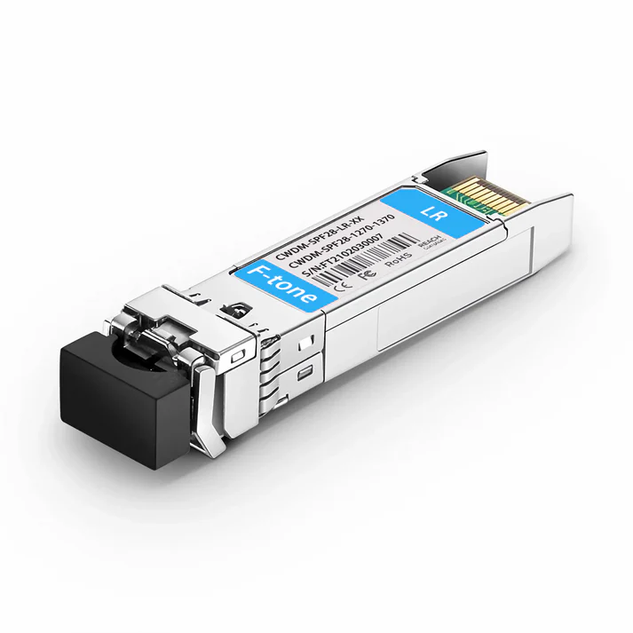
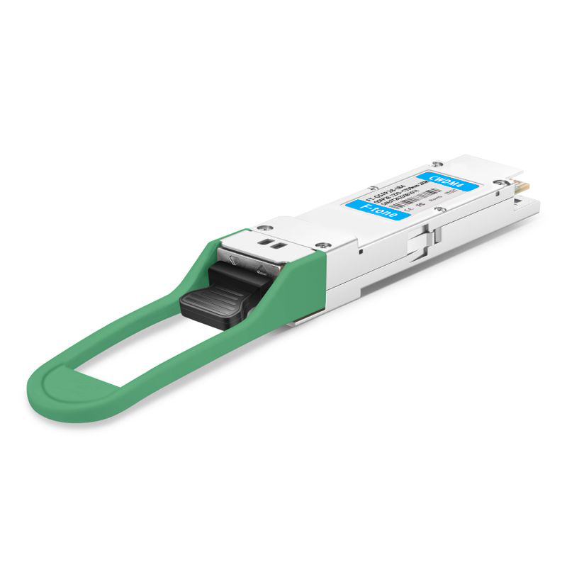
400G QSFP-DD FR4 2km LC Optical Transceiver
This product is a 400Gb/s QSFP-DD optical module designed for 2km optical communication applications. The module converts 8 channels of 50Gb/s (PAM4) electrical input data to 4 channels of CWDM optical signals and multiplexes them into a single channel for 400Gb/s optical transmission.
on the receiver side, the module optically de-multiplexes a 400Gb/s optical input into 4 channels of CWDM optical signals and converts them to 8 channels of 50Gb/s (PAM4) electrical output data.
The central wavelengths of the 4 CWDM channels are 1271,1291,1311 and 1331 nm as members of the CWDM wavelength grid defined in ITU-T G.694.2. Host FEC is required to support up to 2km fiber transmission.
The FQDD-400G-FR4 transceiver is based on proprietary F-tone PLC technology, using surface mounted opto-electronic devices with no free space elements. The unique design of the optical engine facilitates unparalleled compactness while maintaining Telcordia robustness.
Absolute Maximum Ratings
|
Parameter |
Symbol |
Min |
Max |
Units |
|
Storage Temperature Range |
Tsrg |
-40 |
+85 |
℃ |
|
Supply Voltage |
Vcc |
0 |
4 |
V |
|
Relative Humidity |
FH |
10%to 90% non-condensing |
||
Operating Conditions
|
Parameter |
Symbol |
Min |
Max |
Units |
|
Storage Temperature Range |
Tsrg |
-40 |
+85 |
℃ |
|
Supply Voltage |
Vcc |
0 |
4 |
V |
|
Relative Humidity |
FH |
10%to 90% non-condensing |
||
Wavelength Lane Assignments
|
Transmitter Parameter |
Lane |
Min |
Typica |
Max |
Units |
|
Lane Wavelength Range |
Lane 0 Lane 1 Lane 2 Lane 3 |
1264.5 1284.5 1304.5 1324.5 |
1271 1291 1311 1331 |
1277.5 1297.5 1317.5 13375 |
nm nm nm nm |
Transmitter Optical Specifications
|
Transmitter Parameter |
Lane |
Min |
Typical |
Max |
Units |
|
Average launch Power per lane |
|
-3.3 |
|
3.5 |
dBm |
|
Total Average launch power |
|
|
|
9.3 |
dBm |
|
Dutter Optical Modulation Amplitude (OMA outer), each lane |
|
-0.3 |
|
3.7 |
dBm |
|
Difference in launch power between any two lanes (OMA outer) |
|
|
|
4 |
dB |
|
Average Launch Power per Lane @TX Off State |
|
|
|
-20 |
dBm |
|
Launch Power in OMA outer minus TDECQ, each Lane for ER ≥4.5dB for ER<4.5dB |
-1.7 -1.6 |
dBm |
|||
|
Transmitter and Dispersion Eye Closure for PAM4, each Lane |
|
|
|
3.4 |
dB |
|
Extinction Ratio |
|
3.5 |
|
|
dB |
|
Relative Intensity Noise (OMA) |
|
|
|
-136 |
dB/Hz |
|
Side-Mode Suppression Ration (SMSR) |
|
30 |
|
|
dB |
|
Optical Return Loss Tolerance |
|
|
|
17.1 |
dB |
|
Transmitter Reflectance |
|
|
|
-26 |
dB |
|
Transmitter Output Power Monitoring Accuracy |
|
-3 |
|
3 |
dB |
|
TDECQ-10*log10(Ceq), each Lane |
|
|
|
3.4 |
dB |
|
Transmitter transition time |
|
|
|
17 |
ps |
High Speed Electrical Specifications
|
Parameter |
Min |
Typical |
Max |
Units Notes |
|
|
Receiver electrical output characteristics at TP4 |
|||||
|
Signaling rate per lane |
|
26.5625 |
|
GBd |
|
|
AC common-mode output voltage (FMS) |
|
|
17.5 |
mV |
|
|
Differential peak-to-peak output voltage |
|
|
900 |
mV |
|
|
Near-end ESMW (Eye symmetry mask width) |
|
0.265 |
|
UI |
|
|
Near-end Eye height, differential |
70 |
|
|
mV |
|
|
Far-end ESMW (Eye symmetry mask width) |
|
0.2 |
|
UI |
|
|
Far-end Eye height, differential |
30 |
|
|
mV |
|
|
Far-end pre-cursor ISl ratio |
-4.5 |
|
2.5 |
% |
|
|
Differential output return loss |
9.5-0.37f |
|
|
dB |
0.01-8GHz |
|
4.75-7.4log 10 (f/14) |
|
|
dB |
8-19 GHz |
|
|
Common to differential mode conversion return loss |
22-20(f/25.78) |
|
|
dB |
0.01-12.89GHz |
|
15-6log 10 (f/25.78) |
|
|
dB |
12.89-19 GHz |
|
|
Differential termination mismatch |
|
|
10 |
% |
|
|
Transition time (min,20%to 80%) |
9.5 |
|
|
ps |
|
|
DC common mode voltage |
-350 |
|
2850 |
mV |
|
|
Transmitter electrical input characteristics at TP1 |
|||||
|
Signaling rate, per lane |
|
26.5625 |
|
GBd |
|
|
Differential pk-pk input voltage tolerance |
900 |
|
|
mV |
|
|
Differential input return loss |
9.5-0.37f |
|
|
dB |
0.01-8GHz |
|
4.75-7.4log 10 (f/14) |
|
|
dB |
8-19 GHz |
|
|
Differential to common mode input return loss |
22-20(f/25.78) |
|
|
dB |
0.01-12.89GHz |
|
15-6log 10 (f/25.78) |
|
|
dB |
12.89-19 GHz |
|
|
Differential termination mismatch |
|
|
10 |
% |
|
|
Module stressed input test |
Per Section 120E.3.4.1 IEEE802.3bs |
|
|
|
|
|
Single-ended voltage tolerance range |
-0.4 |
|
3.3 |
V |
|
|
Common-mode voltage |
-350 |
|
2850 |
mV |
|
Receiver Output Power Thresholds for Loss of Signal (LOS)
|
Parameter |
Min |
Typica Max |
Units |
|
|
FX_LOS_Assert Min/Max |
-20.0 |
|
dBm |
|
|
FX_LOS_De-Assert Min/Max |
|
|
dBm |
|
|
FX_LOS_Hysteresis |
0.5 |
|
dB |
|
Digital Diagnostic Monitoring Specifications
|
Parameters |
Unit |
Specification |
|
Temperature Monitor absolute error |
degC |
±3 |
|
Voltage Monitor absolute error |
% |
±5 |
|
_bias Monitor absolute error |
% |
±10 |
|
Received Power (Rx)Monitor absolute error |
dB |
±3.0 |
|
Transmit Power (Tx)Monitor absolute error |
dB |
±3.0 |
QSFP-DD Edge Connector and Pinout Description
The electrical pinout of the QSFP-DD module is shown in Figure 2 below.
Figure 1. Host PCB QSFP-DD pad assignment top view
Mechanical Specifications
Ordering information
|
Part Number |
Description |
|
FQDD-400G-FR4 |
400G QSFP-DD FR4 Optical Transceiver |
工作温度:商业级/工业级/军品级可选
本产品为 北亿纤通 | F-tone Networks FT-81系列产品线,详细信息,请联系我们的销售人员,谢谢!Important Notice Performance figures, data and any illustrative material provided in this data sheet are typical and must be specifically confirmed in writing by Andxe System before they become applicable to any particular order or contract. In accordance with the Andxe System policy of continuous improvement specifications may change without notice.The publication of information in this data sheet does not imply freedom from patent or other protective rights of Andxe System or others. Further details are available from any Andxe System sales representative.