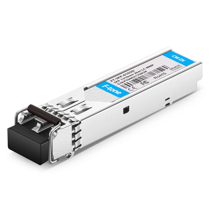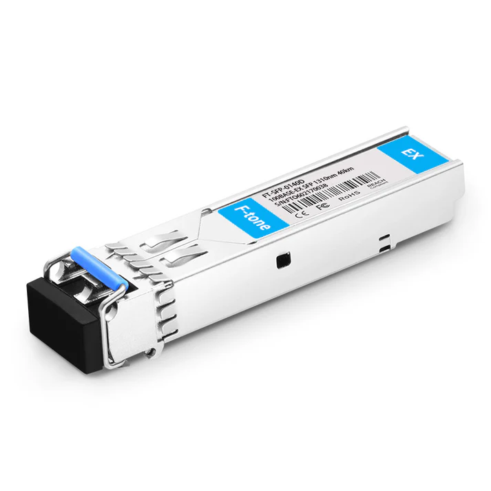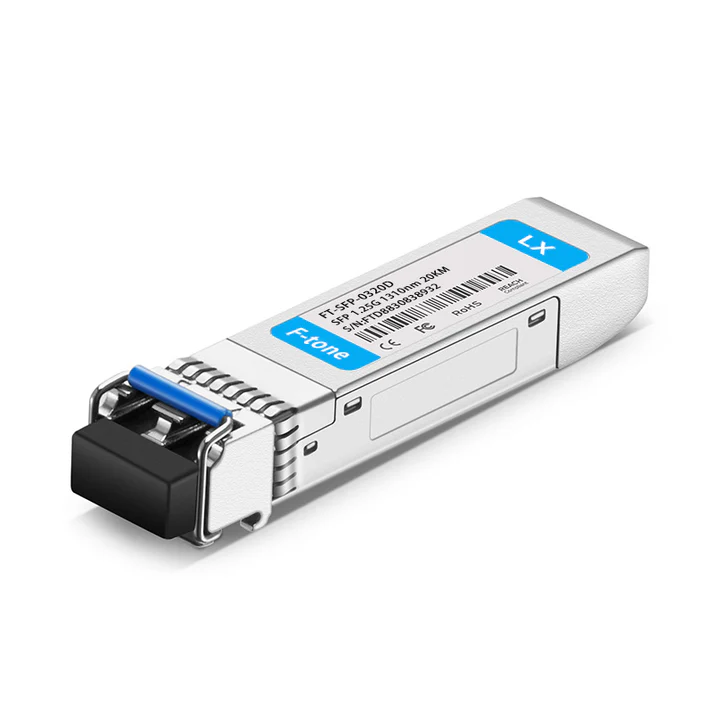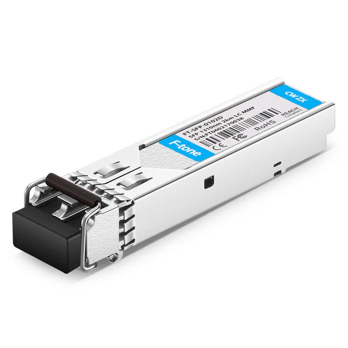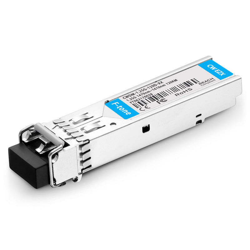
Features:
Up to 1.25Gb/s Data Links
Hot-Pluggable
Single LC connector
Up to 180km on 9/125μm SMF
1550nm DFB laser transmitter
APD Receiver
Single +3.3V Power Supply
Monitoring Interface Compliant with SFF-8472
Power dissipation<1.5W
operating temperature range: 0°C to 70°C
RoHS compliant and Lead Free
Applications:
1000Base-ZX Ethernet
Metro/Access Networks
1×Fibre Channel
Other Optical Links
FSPD-03BD180-5549
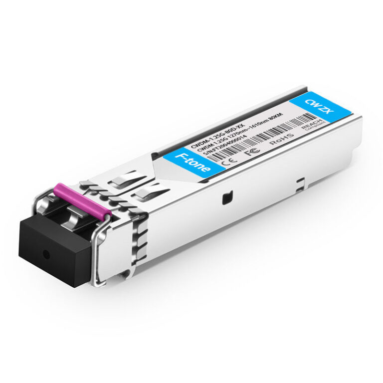
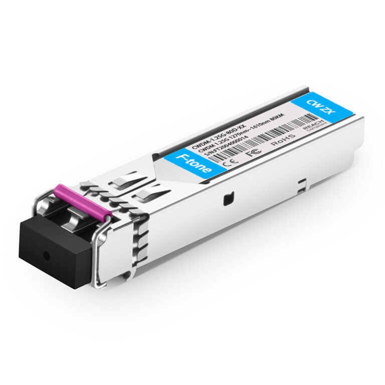
1.25Gb/s 180km LC BiDi SFP Transceiver
Hot Pluggable, Single LC, +3.3V, 1550nm Tx/1490nm Rx, DFB-LD&APD, Single-mode, DDM
Description:
F-tone FSPD-03BD180-5549 Transceivers are a high performance, cost effective module which have a single LC optics interface. They are compatible with the Small Form Factor Pluggable Multi-Sourcing Agreement (MSA) and Digital diagnostics functions are available via the 2-wire serial bus specified in SFF-8472.The receiver section uses a PIN receiver and the transmitter uses a 1550 nm DFB laser, more than 40dB link budge ensure this module 1000Base-ZX Ethernet 180km application.
Absolute Maximum Ratings
|
Parameter |
Symbol |
Min. |
Typical |
Max. |
Unit |
|
Storage Temperature |
TS |
-40 |
|
+85 |
°C |
|
Supply Voltage |
VCC |
-0.5 |
|
4 |
V |
|
Relative Humidity |
FH |
0 |
|
85 |
% |
Recommended Operating Environment:
|
Parameter |
Symbol |
Min. |
Typical |
Max. |
Unit |
|
Case operating Temperature |
TC |
0 |
|
+70 |
°C |
|
Supply Voltage |
VCC |
3.1 |
|
3.6 |
V |
|
Supply Current |
Icc |
|
|
300 |
mA |
|
Inrush Current |
Isurge |
|
|
Icc+30 |
mA |
|
Power dissipation |
Pmax |
|
|
1.5 |
W |
Electrical Characteristics TOP=(TOP=-30 to70°C, VCC = 3.1 to 3.6 Volts)
|
Parameter |
Symbol |
Min. |
Typical |
Max. |
Unit |
Note |
|
Transmitter Section: |
|
|||||
|
Input differential impedance |
Rin |
90 |
100 |
110 |
|
|
|
Single ended data input swing |
Vin PP |
250 |
|
1200 |
mVp-p |
|
|
Transmit Disable Voltage |
VD |
Vcc – 1.3 |
|
Vcc |
V |
2 |
|
Transmit Enable Voltage |
VEN |
Vee |
|
Vee+ 0.8 |
V |
|
|
Transmit Disable Assert Time |
Tdessert |
|
|
10 |
us |
|
|
Receiver Section: |
|
|||||
|
Single ended data output swing |
Vout,pp |
300 |
|
800 |
mv |
3 |
|
LOS Fault |
Vlosfault |
Vcc – 0.5 |
|
VCC_host |
V |
5 |
|
LOS Normal |
Vlos norm |
Vee |
|
Vee+0.5 |
V |
5 |
|
Power Supply Rejection |
PSR |
100 |
|
|
mVpp |
6 |
Note:
1.AC coupled.
2.Or open circuit.
3.Into 100 ohm differential termination.
4.20 – 80 %
5.LOS is LVTTL. Logic 0 indicates normal operation; logic 1 indicates no signal detected.
6. All transceiver specifications are compliant with a power supply sinusoidal modulation of 20 Hz to 1.5MHz up to specified value applied through the power supply filtering network shown on page 23 of the Small Form-factor Pluggable (SFP) Transceiver Multi-Source Agreement (MSA), September 14, 2000.
Optical Parameters(TOP=-30 to70°C, VCC = 3.1 to 3.6 Volts)
|
Parameter |
Symbol |
Min. |
Typical |
Max. |
Unit |
Note |
|
Transmitter Section: |
||||||
|
Center Wavelength |
λc |
1530 |
1550 |
1570 |
nm |
|
|
Spectral Width(FMS) |
σRMS |
|
|
4 |
nm |
|
|
Optical Output Power |
Pout |
+3 |
|
+6 |
dBm |
1 |
|
Extinction Ratio |
ER |
8.2 |
|
|
dB |
|
|
Optical Rise/Fall Time |
tr/ tf |
|
|
260 |
ps |
2 |
|
Relative Intensity Noise |
FIN |
|
|
-120 |
dB/Hz |
|
|
Total Jitter Contribution |
TXΔ TJ |
|
|
0.284 |
UI |
3 |
|
Eye Mask for Optical Output |
Compliant with IEEE802.3 z (class 1 laser safety) |
|
||||
|
Receiver Section: |
|
|||||
|
Optical Input Wavelength |
λc |
1470 |
1490 |
1510 |
nm |
|
|
Receiver Overload |
Pol |
-7 |
|
|
dBm |
4 |
|
FX Sensitivity |
Sen |
|
|
-37 |
dBm |
4 |
|
FX_LOS Assert |
LOSA |
-45 |
|
|
dBm |
|
|
FX_LOS De-assert |
LOSD |
|
|
-37 |
dBm |
|
|
FX_LOS Hysteresis |
LOSH |
0.5 |
|
|
dB |
|
|
General Specifications: |
||||||
|
Data Rate |
BR |
|
1.25 |
|
Gb/s |
|
|
Bit Error Rate |
BER |
|
|
10-12 |
|
|
|
Max. Supported Link Length on 9/125μm SMF@1.25Gb/s |
LMAX |
|
180 |
|
km |
|
|
Total System Budget |
LB |
40 |
|
|
dB |
|
Note
1.The optical power is launched into SMF.
2.20-80%.
3.Contributed total jitter is calculated from DJ and FJ measurements using TJ = FJ + DJ. Contributed FJ is calculated for 1×10-12 BER by multiplying the FMS jitter (measured on a single rise or fall edge) from the oscilloscope by 14. Per FC-PI (Table 9 – SM jitter output, note 1), the actual contributed FJ is allowed to increase above its limit if the actual contributed DJ decreases below its limits, as long as the component output DJ and TJ remain within their specified FC-PI maximum limits with the worst case specified component jitter input.
4.Measured with PRBS 27-1at 10-12BER
Pin Assignment
Diagram of Host Board Connector Block Pin Numbers and Name
Diagram of Host Board Connector Block Pin Numbers and Names
Pin Function Definitions
|
Pin No |
Name |
Function |
Plug Seq |
Notes |
|
1 |
VeeT |
Transmitter Ground |
1 |
1 |
|
2 |
TX Fault |
Transmitter Fault Indication |
3 |
|
|
3 |
TX Disable |
Transmitter Disable |
3 |
2 |
|
4 |
MOD-DEF2 |
Module Definition |
2 |
3 |
|
5 |
MOD-DEF1 |
Module Definition 1 |
3 |
3 |
|
6 |
MOD-DEF0 |
Module Definition 0 |
3 |
3 |
|
7 |
Rate Select |
Not Connected |
3 |
4 |
|
8 |
LOS |
Loss of Signal |
3 |
5 |
|
9 |
VeeR |
Receiver Ground |
1 |
1 |
|
10 |
VeeR |
Receiver Ground |
1 |
1 |
|
11 |
VeeR |
Receiver Ground |
|
1 |
|
12 |
FT- |
Inv. Received Data Out |
3 |
6 |
|
13 |
FD+ |
Received Data Out |
3 |
6 |
|
14 |
VeeR |
Receiver Ground |
3 |
1 |
|
15 |
VccR |
Receiver Power |
2 |
1 |
|
16 |
VccT |
Transmitter Power |
2 |
|
|
17 |
VeeT |
Transmitter Ground |
1 |
|
|
18 |
TD+ |
Transmit Data In |
3 |
6 |
|
19 |
TD- |
Inv. Transmit In |
3 |
6 |
|
20 |
VeeT |
Transmitter Ground |
1 |
|
Notes:
1. Circuit ground is internally isolated from chassis ground.
2. Laser output disabled on TDIS >2.0V or open, enabled on TDIS <0.8V.
3. Should be pulled up with 4.7k – 10 kohms on host board to a voltage between 2.0V and 3.6V.MOD_DEF(0) pulls line low to indicate module is plugged in.
4. Rate select is not used
5. LOS is open collector output. Should be pulled up with 4.7k – 10 kohms on host board to a voltage between 2.0V and 3.6V. Logic 0 indicates normal operation; logic 1 indicates loss of signal.
6. AC Coupled
Recommended Circuit
SFP Host Recommended Circuit
Mechanical Dimensions
Mechanical Drawing
工作温度:商业级/工业级/军品级可选
本产品为 北亿纤通 | F-tone Networks FT-81系列产品线,详细信息,请联系我们的销售人员,谢谢!Important Notice Performance figures, data and any illustrative material provided in this data sheet are typical and must be specifically confirmed in writing by Andxe System before they become applicable to any particular order or contract. In accordance with the Andxe System policy of continuous improvement specifications may change without notice.The publication of information in this data sheet does not imply freedom from patent or other protective rights of Andxe System or others. Further details are available from any Andxe System sales representative.